
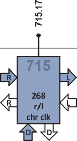
Node 715
This node functions alternatively as a wire node, passing data from 714 to 716, and as a character clock signal generator.
Source code
715 char clock, r/l
go 00 @ ! b! @b drop b! !b drop go ; 03
init 1F5 r-l- a! 0 20000 io down 0 30000 io down
dup dup drop drop go ; 11
7 r 0 u 0 ether
go 00 @ ! b! @b drop b! !b drop go ; 03
init 1F5 r-l- a! 0 20000 io down 0 30000 io down
dup dup drop drop go ; 11
7 r 0 u 0 ether
Definitions
- go
- First read a word from RIGHT and send it to LEFT. Then suspend reading from DOWN. A word read from DOWN is a signal to toggle GPIO 715.17 pin level. Repeat these two steps indefinitely.
- init
- Set register A, prefill stack with addresses and output values, and jump to go.
Description
This node combines two functions. It is a wire passing data from node 714 to 716; it also toggles GPIO pin 715.17 when a signal is received from character clock via node 615. Note that the node suspends while waiting for a next clock signal. When pin 17 toggles, all three analog nodes generating VGA color components receive this clock edge at the same time.